- 您现在的位置:买卖IC网 > Sheet目录2000 > IDT5T940-10NLGI (IDT, Integrated Device Technology Inc)IC CLK GENERATOR PREC 28-VFQFPN
7
INDUSTRIALTEMPERATURERANGE
IDT5T940
PRECISION CLOCKGENERATOROC-192APPLICATIONS
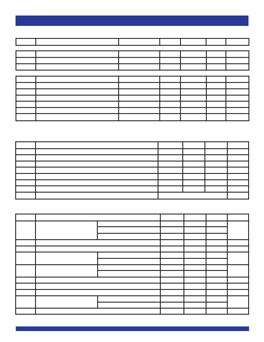
INPUT TIMING REQUIREMENTS
Symbol
Parameter
Min.
Typ.
Max.
Unit
REFH
Input Reference Clock Duty Cycle
40
50
60
%
FREF
InputReferenceClockRange
19.44
—
666.52
MHz
REFTOL
InputReferenceClockFrequencyTolerance
-100
—
100
ppm
FCLKIN
Clock in Frequency Range
19.44
—
666.52
MHz
CLKINH
Clock in Duty Cycle
40
50
60
%
tAQ
Acquisition Time from Return of Valid CLKIN
—
60
150
us
LOCKTOL
FrequencyToleranceforLOCK
-600
±450
600
ppm
tJIT(TOL)
TolerancetoInputJitter
GR-253 Sect. 5.6.2.2
Symbol
Parameter
Min.
Typ.
Max.
Unit
SELmode = LOW
155.52
—
166.63
QOUT
MultipliedClockOutputFrequency
SELmode = MID
155.52
—
666.52
MHz
SELmode = HIGH
622.08
—
666.52
QREG
RegeneratedClockOutputFrequency
19.44
—
666.52
MHz
CLKIN
Input Clock Frequency
19.44
—
667
MHz
tR
OutputRiseTime
LVPECL
—
150
—
ps
LVDS
—
100
—
tF
OutputFallTime
LVPECL
—
150
—
ps
LVDS
—
100
—
tSK
Skew between QOUT and QREG
—
10
20
ps
PLLBW
PLLBandwidthSetting
65
80
120
KHz
tP
JitterTransferPeaking
——
0.1
dB
tJ
JitterGeneration(1)
Output Frequency = 622MHz - 666.5MHz
—
0.3
0.65
ps (RMS)
(with 50KHz to 80MHz band pass filter)
Output Frequency = 155.5MHz - 166.6MHz
—
1
2
tDUTY
Output Duty Cycle
45
—
55
%
AC ELECTRICAL CHARACTERISTICS OVER OPERATING RANGE (OC-192)
NOTE:
1. All input frequencies and PLLBW[1:0] permitted by PLL Bandwidth Selection table.
DC ELECTRICAL CHARACTERISTICS OVER OPERATING RANGE FOR LVDS
Symbol
Parameter
Test Conditions
Min.
Typ.
Max.
Unit
InputCharacteristics
IIN
Input Current (CLKIN, REFIN)
VDD = 3.465V
-20
—
+20
μA
VCM
CommonModeInputVoltageRange(1)
0.9
—
VDD - 0.05
V
VDIF
DifferentialVoltageRequiredtoToggleInput
100
——
mV
OutputCharacteristics
VOT(+)
DifferentialOutputVoltagefortheTRUEBinaryState
247
—
454
mV
VOT(-)
DifferentialOutputVoltagefortheFALSEBinaryState
-247
—
-454
mV
ΔVOT
Change in VOTBetweenComplementaryOutputStates
——
50
mV
VOS
OutputCommonModeVoltage(OffsetVoltage)
1.125
1.2
1.375
V
ΔVOS
Change in VOSBetweenComplementaryOutputStates
——
50
mV
IOS
OutputsShortCircuitCurrent
VOUT(+) and VOUT(-) = 0V
—
924
mA
IOSD
DifferentialOutputsShortCircuitCurrent
VOUT(+) = VOUT(-)
—
612
mA
NOTE:
1. Not to exceed VDD - 0.05V.
发布紧急采购,3分钟左右您将得到回复。
相关PDF资料
IDT5T9820NLI8
IC CLK DRIVER ZD PLL 68-VFQFPN
IDT5T9890NLI8
IC CLK DRIVER 2.5V PLL 68-VFQFPN
IDT5V19EE604NDGI8
IC PLL CLK GEN 200MHZ 28VFQFPN
IDT5V40501DVG
IC CLK GEN PLL 160MHZ 8TSSOP
IDT5V41064NLGI
IC CLK GEN 1:1 16QFN
IDT5V41066PGG
IC CLK GEN SPRED SPECTRM 20TSSOP
IDT5V49EE901NLGI8
IC PLL CLK GEN 200MHZ 32VFQFN
IDT5V49EE902NLGI
IC CLOCK GEN PLL 500MHZ 32VFQFPN
相关代理商/技术参数
IDT5T940-10NLGI8
功能描述:IC CLK GENERATOR PREC 28-VFQFPN RoHS:是 类别:集成电路 (IC) >> 时钟/计时 - 专用 系列:- 标准包装:1,500 系列:- 类型:时钟缓冲器/驱动器 PLL:是 主要目的:- 输入:- 输出:- 电路数:- 比率 - 输入:输出:- 差分 - 输入:输出:- 频率 - 最大:- 电源电压:3.3V 工作温度:0°C ~ 70°C 安装类型:表面贴装 封装/外壳:28-SSOP(0.209",5.30mm 宽) 供应商设备封装:28-SSOP 包装:带卷 (TR) 其它名称:93786AFT
IDT5T940-30NLGI
功能描述:IC CLK GENERATOR PREC 28-VFQFPN RoHS:是 类别:集成电路 (IC) >> 时钟/计时 - 专用 系列:- 标准包装:1 系列:- 类型:时钟/频率发生器,多路复用器 PLL:是 主要目的:存储器,RDRAM 输入:晶体 输出:LVCMOS 电路数:1 比率 - 输入:输出:1:2 差分 - 输入:输出:无/是 频率 - 最大:400MHz 电源电压:3 V ~ 3.6 V 工作温度:0°C ~ 85°C 安装类型:表面贴装 封装/外壳:16-TSSOP(0.173",4.40mm 宽) 供应商设备封装:16-TSSOP 包装:Digi-Reel® 其它名称:296-6719-6
IDT5T940-30NLGI8
功能描述:IC CLK GENERATOR PREC 28-VFQFPN RoHS:是 类别:集成电路 (IC) >> 时钟/计时 - 专用 系列:- 标准包装:1,500 系列:- 类型:时钟缓冲器/驱动器 PLL:是 主要目的:- 输入:- 输出:- 电路数:- 比率 - 输入:输出:- 差分 - 输入:输出:- 频率 - 最大:- 电源电压:3.3V 工作温度:0°C ~ 70°C 安装类型:表面贴装 封装/外壳:28-SSOP(0.209",5.30mm 宽) 供应商设备封装:28-SSOP 包装:带卷 (TR) 其它名称:93786AFT
IDT5T9820NLGI
功能描述:IC CLK DRIVER ZD PLL 68-VFQFPN RoHS:是 类别:集成电路 (IC) >> 时钟/计时 - 时钟发生器,PLL,频率合成器 系列:- 标准包装:39 系列:- 类型:* PLL:带旁路 输入:时钟 输出:时钟 电路数:1 比率 - 输入:输出:1:10 差分 - 输入:输出:是/是 频率 - 最大:170MHz 除法器/乘法器:无/无 电源电压:2.375 V ~ 3.465 V 工作温度:0°C ~ 70°C 安装类型:* 封装/外壳:* 供应商设备封装:* 包装:*
IDT5T9820NLGI8
功能描述:IC CLK DRIVER ZD PLL 68-VFQFPN RoHS:是 类别:集成电路 (IC) >> 时钟/计时 - 时钟发生器,PLL,频率合成器 系列:- 标准包装:39 系列:- 类型:* PLL:带旁路 输入:时钟 输出:时钟 电路数:1 比率 - 输入:输出:1:10 差分 - 输入:输出:是/是 频率 - 最大:170MHz 除法器/乘法器:无/无 电源电压:2.375 V ~ 3.465 V 工作温度:0°C ~ 70°C 安装类型:* 封装/外壳:* 供应商设备封装:* 包装:*
IDT5T9820NLI
功能描述:IC CLK DRIVER ZD PLL 68-VFQFPN RoHS:否 类别:集成电路 (IC) >> 时钟/计时 - 时钟发生器,PLL,频率合成器 系列:- 标准包装:39 系列:- 类型:* PLL:带旁路 输入:时钟 输出:时钟 电路数:1 比率 - 输入:输出:1:10 差分 - 输入:输出:是/是 频率 - 最大:170MHz 除法器/乘法器:无/无 电源电压:2.375 V ~ 3.465 V 工作温度:0°C ~ 70°C 安装类型:* 封装/外壳:* 供应商设备封装:* 包装:*
IDT5T9820NLI8
功能描述:IC CLK DRIVER ZD PLL 68-VFQFPN RoHS:否 类别:集成电路 (IC) >> 时钟/计时 - 时钟发生器,PLL,频率合成器 系列:- 标准包装:39 系列:- 类型:* PLL:带旁路 输入:时钟 输出:时钟 电路数:1 比率 - 输入:输出:1:10 差分 - 输入:输出:是/是 频率 - 最大:170MHz 除法器/乘法器:无/无 电源电压:2.375 V ~ 3.465 V 工作温度:0°C ~ 70°C 安装类型:* 封装/外壳:* 供应商设备封装:* 包装:*
IDT5T9821NLGI
功能描述:IC CLK DRIVER ZD PLL 68-VFQFPN RoHS:是 类别:集成电路 (IC) >> 时钟/计时 - 时钟发生器,PLL,频率合成器 系列:- 标准包装:39 系列:- 类型:* PLL:带旁路 输入:时钟 输出:时钟 电路数:1 比率 - 输入:输出:1:10 差分 - 输入:输出:是/是 频率 - 最大:170MHz 除法器/乘法器:无/无 电源电压:2.375 V ~ 3.465 V 工作温度:0°C ~ 70°C 安装类型:* 封装/外壳:* 供应商设备封装:* 包装:*